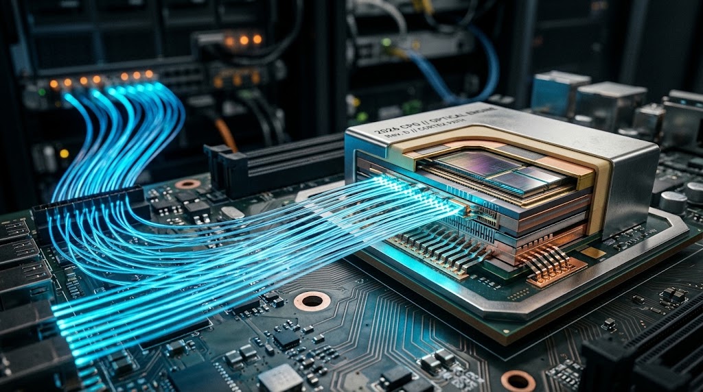
AI racks are reaching power densities once associated with entire rows of conventional servers, while switch bandwidth is exploding into the hundreds of terabits per second. Copper is not disappearing—but at the most bandwidth-intensive points in the AI network, electrical links are being pushed aside by silicon photonics and co-packaged optics.
Published: September 16, 2026
The End of Copper? How Silicon Photonics Is Rewiring the AI Data Center in 2026
AI racks are pushing beyond 100 kW while network switches are moving from 51.2 to 102.4 terabits per second and beyond. The next infrastructure bottleneck is no longer only computation. It is moving data between chips without wasting enormous amounts of electricity—and the industry's answer is increasingly light.
By Deep Tech & Infrastructure Desk | September 16, 2026
If you want to understand where the next major AI hardware breakthrough is happening, do not look only at the GPU.
Look at the few centimetres surrounding it.
Look at the switch ASIC.
Look at the circuit board traces.
Look at the transceivers sitting at the front of the rack.
And then look at the fibre.
Modern AI computers have become so fast that moving information between processors is turning into one of the industry's hardest physical problems.
A GPU can perform astonishing amounts of computation.
But a training cluster only works if thousands—or eventually hundreds of thousands—of accelerators can exchange enormous volumes of data without sitting idle waiting for the network.
That requirement is colliding with basic physics.
Electrical signals travelling through copper lose quality as:
bandwidth rises,
distance increases,
and signal frequencies climb.
Engineers compensate with stronger SerDes, equalization, retimers and digital signal processors.
But those fixes consume electricity.
They add latency.
They generate heat.
And eventually the cost of preserving an electrical signal becomes harder to justify than converting the information into light.
That is why 2026 is becoming a pivotal year for silicon photonics and co-packaged optics, or CPO.
TSMC says its first true co-packaged-optics implementation using its COUPE photonics technology is scheduled to begin production in 2026. Broadcom is shipping 102.4-Tb/s switch silicon and offering a CPO version built around TSMC's photonics technology. NVIDIA says its Spectrum-X Ethernet Photonics platform has moved into production alongside the Vera Rubin generation.
This is not the end of copper everywhere.
It is something more precise—and arguably more important:
the point at which light begins moving substantially closer to the processor.
The AI Bottleneck Has Moved From Computation to Communication
Traditional computing workloads often allow processors to spend much of their time working independently.
Large AI training systems behave differently.
Training a frontier model may distribute one workload across:
thousands of GPUs,
multiple racks,
multiple network switches,
and sometimes multiple buildings.
The processors constantly exchange:
model parameters,
gradients,
activation data,
expert-routing traffic,
and synchronization messages.
If one part of that network slows down, expensive accelerators can sit idle.
That is a terrible economic outcome.
A modern AI accelerator may consume more than a kilowatt of power.
An entire rack can now reach roughly 120 kW, according to a 2026 NVIDIA GTC presentation on next-generation AI power infrastructure. The same presentation describes future rack designs potentially heading toward much higher densities.
At those densities, every additional watt consumed by networking matters.
Not because networking alone determines rack power—
but because an AI facility containing thousands of racks multiplies small inefficiencies into megawatts.
Two Different Copper Problems Are Happening at the Same Time
This distinction is crucial.
Modern AI data centres are confronting two separate physical problems involving copper.
Power distribution
Racks drawing 100 kW or more require enormous electrical current when delivered at relatively low voltages.
That makes conductors:
thicker,
heavier,
hotter,
and harder to route.
The power industry is therefore exploring higher-voltage architectures, including 800-volt DC systems, to reduce current and conductor mass in future AI infrastructure.
Data communication
At the same time, increasingly fast electrical links between chips, boards and switches face:
signal attenuation,
crosstalk,
equalization requirements,
retimer power,
and distance limitations.
This is the problem silicon photonics attacks.
CPO does not replace the copper busbars feeding electricity to a GPU rack.
It replaces or shortens some of the most demanding electrical data paths.
The future AI data centre may therefore undergo two transitions simultaneously:
higher-voltage electricity carries the power
while
light carries more of the data.
Why Copper Becomes Difficult at Extreme Bandwidth
Copper is remarkably good.
It is inexpensive.
Reliable.
Easy to manufacture.
Easy to repair.
And for sufficiently short distances, highly efficient.
That is why it will remain inside computing systems for a long time.
Broadcom's own Tomahawk 6—the company's 102.4-Tb/s AI-networking switch—still advertises long-reach passive copper support through its 100G and 200G SerDes.
So why move to optics?
Because electrical links become progressively harder as bit rates increase.
A high-speed electrical signal is not a perfect stream of ones and zeros.
It is an analog electromagnetic waveform.
As it moves through:
circuit-board traces,
connectors,
cables,
vias,
and packages,
the signal degrades.
Loss increases with frequency.
Reflections distort the waveform.
Neighbouring traces interfere.
Timing margins shrink.
The receiver has to reconstruct the original data from an increasingly ugly electrical signal.
Engineers compensate using:
equalization,
forward error correction,
retimers,
DSPs,
and increasingly sophisticated SerDes.
That engineering is extraordinary.
But it costs power.
And the closer the industry gets to 200 gigabits per second per electrical lane, the more attractive it becomes to shorten the electrical journey dramatically.
Optical Fibre Has a Different Scaling Advantage
Fibre carries information as photons rather than electrical current flowing through a conductor.
That brings several important advantages.
Optical fibre can support:
very high bandwidth,
longer reach,
low signal attenuation,
much lower sensitivity to electromagnetic interference,
and a much smaller cable cross-section for enormous aggregate bandwidth.
This is why fibre already dominates:
telecommunications,
data-centre interconnects,
and long-distance networking.
The problem historically was not whether optics worked.
It was where the electrical-to-optical conversion happened.
For decades, that conversion lived primarily in a pluggable optical module at the front edge of a switch.
CPO changes the location.
How a Traditional Optical Switch Works
Imagine a conventional high-performance Ethernet switch.
At its centre is a switch ASIC.
Packets arrive.
The ASIC decides where they should go.
But the ASIC itself speaks electrically.
So data leaves the silicon through high-speed electrical SerDes.
It travels:
through the package,
across circuit-board traces,
toward the front panel.
There, a pluggable optical transceiver converts the electrical signal into light.
The light then enters fibre.
This architecture has enormous advantages.
The optical modules are replaceable.
They can be serviced independently.
Different optics can be installed for different link lengths.
And decades of networking infrastructure have evolved around this modular model.
But as switch bandwidth rises, the electrical distance between the ASIC and the optics becomes increasingly expensive in both signal integrity and power.
The board trace has become the problem.
Co-Packaged Optics Moves the Conversion Point
CPO changes the architecture.
Instead of placing the optical engine at the front edge of the board, the photonic engines sit extremely close to the switch ASIC—often on the same package substrate.
The long high-speed electrical trace largely disappears.
Electrical data travels only a tiny distance.
Then it becomes light.
The fibre carries it the rest of the way.
Conceptually:
Traditional architecture
switch silicon
→ electrical SerDes
→ long PCB trace
→ pluggable transceiver
→ optical fibre
CPO
switch silicon
→ very short electrical connection
→ co-packaged photonic engine
→ optical fibre
That shorter electrical path is the key.
What Exactly Is Silicon Photonics?
Traditional optical systems use specialized optical components to:
generate,
modulate,
route,
and detect light.
Silicon photonics moves many of those functions onto silicon-compatible semiconductor structures.
Instead of treating optical hardware as a completely separate technology, manufacturers can integrate:
waveguides,
modulators,
photodetectors,
and electronic control circuitry
using semiconductor-style manufacturing and advanced packaging.
The laser itself does not necessarily need to be fabricated directly in silicon.
In many architectures, the light source uses III-V semiconductor materials such as indium phosphide and can remain external or replaceable.
That is an important correction to the popular claim that companies are simply:
“putting lasers inside GPUs.”
The real architecture is more sophisticated.
Electronic compute or switching silicon sits extremely close to photonic engines that manipulate externally supplied or integrated laser light.
TSMC's COUPE Is One of the Most Important Pieces
TSMC calls its silicon-photonics platform:
Compact Universal Photonic Engine, or COUPE.
The manufacturing challenge is not merely creating optical components.
The real challenge is integrating photonics with advanced electronic logic at extremely high density.
TSMC uses its SoIC-X 3D stacking technology to place an electrical die directly above a photonic die.
TSMC says this architecture offers a low-impedance die-to-die interface and improved energy efficiency compared with conventional approaches.
That means one layer can perform:
electrical control,
signal processing,
and driver functions,
while another handles:
optical modulation,
light routing,
and photodetection.
The vertical connection between them is microscopic.
That is the kind of integration CPO requires.
2026 Is the Production Year TSMC Has Been Pointing Toward
TSMC originally laid out a roadmap that would:
qualify COUPE for compact pluggable optics,
then bring COUPE into advanced packaging for true co-packaged optics.
At its 2026 North America Technology Symposium, TSMC said COUPE-on-substrate co-packaged optics is beginning production in 2026.
TSMC claims this approach provides:
2× better power efficiency
and
10× lower latency
compared with a pluggable implementation located on the circuit board.
Those figures are TSMC's own platform comparisons, not a universal law applying to every optical network.
But they illustrate why hyperscalers care.
At AI-factory scale, watts saved per optical link multiply across an extraordinary number of connections.
Broadcom Has Already Taken the Switch to 102.4 Tbps
Now consider the bandwidth involved.
Broadcom's Tomahawk 6 delivers:
102.4 terabits per second
of switching capacity in a single switch ASIC.
Broadcom began shipping the Tomahawk 6 family in production volume in March 2026.
To visualize 102.4 Tb/s:
that is more than 100 trillion bits every second moving through one switching device.
The chip supports:
100G and 200G SerDes,
scale-up networking,
scale-out networking,
and an optional CPO implementation.
This is precisely where optics becomes compelling.
Sending 102.4 Tb/s from one ASIC toward dozens or hundreds of external optical modules using long high-speed electrical traces becomes an extraordinary board-design problem.
Move the optics next to the switch—
and much of that electrical journey disappears.
Tomahawk 6 Davisson Shows What CPO Looks Like Commercially
Broadcom's CPO version is called Tomahawk 6 Davisson.
It combines a 102.4-Tb/s Ethernet switch with 16 optical engines, each delivering 6.4 Tb/s.
Those engines use TSMC COUPE technology.
Broadcom says the design reduces optical-interconnect power consumption by around:
70%
relative to traditional pluggable solutions—
equivalent to more than a 3.5× reduction in that portion of network power.
Again, that does not mean an entire AI rack suddenly uses 70% less power.
The claim applies to the optical interconnect portion.
That distinction matters.
But at hyperscale, reducing network power by even a few watts per high-speed link is enormously valuable.
CPO Is About Reliability as Much as Electricity
There is another hidden problem in giant AI networks.
A single network interruption can stall an enormous distributed training workload.
Imagine 50,000 GPUs cooperating on one job.
If part of the fabric repeatedly loses links, the cost is not merely replacing one transceiver.
The real cost is wasted accelerator time.
Broadcom argues that integrating optical engines beside the switch eliminates many sources of variability associated with:
long electrical traces,
pluggable-module interfaces,
signal conditioning,
and complex front-panel electronics.
NVIDIA makes a similar argument.
It says its CPO systems deliver substantially greater network resiliency and longer uninterrupted AI workload execution compared with conventional pluggable designs.
In a million-GPU-scale future, uptime can be worth more than the optical hardware itself.
NVIDIA Has Pushed the Idea Even Further
Broadcom's 102.4-Tb/s switch is not the end of the bandwidth race.
NVIDIA's 2026 Spectrum-X Ethernet Photonics platform shows how quickly the numbers are escalating.
Its SN6800 system is specified for:
409.6 Tb/s aggregate bandwidth
with:
512 ports at 800 Gb/s
or
2,048 ports at 200 Gb/s.
NVIDIA says the architecture integrates silicon photonics with the switching ASIC and removes the need for some external DSP retiming.
The company claims approximately:
5× better network power efficiency
and
higher resiliency
compared with traditional pluggable-transceiver networks.
The platform entered production in 2026 as part of NVIDIA's Vera Rubin infrastructure rollout.
So the optical transition is no longer merely a laboratory roadmap.
Commercial AI networking products are appearing now.
102.4 Tbps and 409.6 Tbps Are Not Contradictory
These numbers can easily confuse readers.
Broadcom says:
102.4 Tb/s.
NVIDIA says:
409.6 Tb/s.
Which one is the actual next-generation switch speed?
Both figures can be correct because they refer to different architectural levels and implementations.
Broadcom's Tomahawk 6 figure refers to the switching capacity of a single switch ASIC.
NVIDIA's SN6800 figure refers to the aggregate capacity of a larger switch system built from multiple switching resources.
This distinction matters when comparing AI-network hardware.
Marketing numbers often describe different layers:
per lane,
per port,
per ASIC,
per chassis,
or per fabric.
The unit may be the same.
The object being measured is not.
Why Pluggable Optics Will Not Disappear Overnight
If CPO is so efficient, why hasn't every data centre already switched?
Because pluggable optics have one gigantic advantage:
you can unplug them.
If a transceiver fails, a technician removes it.
The switch remains installed.
That modularity is incredibly valuable.
With co-packaged optics, optical components sit much closer to extremely expensive switching silicon.
That raises difficult engineering questions.
What happens when one laser fails?
How do you replace a photonic engine without discarding a huge switch package?
How do you test optical components before final assembly?
How do technicians service fibre connections in dense racks?
What happens to manufacturing yield if one optical element is defective?
CPO solves one problem while making serviceability much harder.
The External Laser Source Is One Answer
One architectural solution is to keep the laser itself outside the main package.
The photonic engine can contain:
modulators,
waveguides,
and detectors,
while light arrives from an external laser source.
Broadcom's Davisson platform uses field-replaceable external laser modules.
That matters because laser devices can age.
If the laser sits deep inside a huge co-packaged switch and fails, repair becomes difficult.
If the laser remains modular, technicians can replace it independently.
So the commercial version of CPO is not:
seal everything permanently inside one giant chip.
It is a carefully chosen boundary between:
what should be integrated
and
what should remain replaceable.
Why AI Is Forcing This Transition Faster Than Ordinary Cloud Computing Did
Cloud data centres have used optical networking for years.
So why is CPO suddenly urgent?
Because AI changes the traffic pattern.
Traditional cloud applications often communicate primarily between:
servers,
storage,
and users.
Large AI jobs create huge east-west traffic flows inside the compute cluster itself.
Thousands of accelerators repeatedly exchange data with one another.
This creates an unusual requirement:
extremely high bandwidth
with
extremely low latency
and
extremely high reliability.
A single GPU is extraordinarily expensive.
An idle GPU is wasted capital.
The network therefore stops being peripheral infrastructure.
It becomes part of the computer.
The Data Centre Is Becoming One Giant Computer
This may be the most important conceptual change.
A conventional server is a computer.
A rack is a collection of computers.
A data centre is a building full of computers.
AI increasingly breaks that mental model.
A giant training cluster behaves more like:
one computer spread across an entire building.
The GPUs are compute units.
The network is effectively the backplane.
HBM is distributed memory.
Optical links become something resembling enormously extended chip interconnects.
Once you think about the system that way, CPO becomes easier to understand.
If the entire building behaves like one computer, communication between racks cannot remain an afterthought.
Eventually Light May Move Even Closer to the GPU
Today's commercial CPO focus is especially visible around network switches.
But the long-term photonics race goes deeper.
Engineers are exploring optical connectivity at progressively smaller distances:
rack to rack,
switch to switch,
board to board,
package to package,
chiplet to chiplet,
and potentially eventually deeper inside compute systems.
This is sometimes described as moving from:
optical I/O
toward
optical fabrics.
The goal is not necessarily to perform arithmetic with photons.
That is a separate field sometimes called photonic computing.
The near-term revolution is more practical:
keep computing electronically, but move the information optically.
That distinction is important.
CPO is not replacing GPUs with light-based processors.
It is changing how conventional silicon communicates.
Does Light Really Eliminate Heat?
No.
Another common exaggeration.
Optical networking still consumes electricity.
Lasers require power.
Modulators require drivers.
Photodetectors need electronics.
Switch ASICs remain extremely hot.
Optical packages need cooling.
NVIDIA's CPO switches themselves use liquid cooling.
Silicon photonics therefore does not make the network thermally free.
Its advantage is that optical transmission can move enormous bandwidth with less energy per bit over useful distances than increasingly difficult high-speed electrical links.
It reduces one contributor to the thermal problem.
It does not repeal thermodynamics.
And Copper Is Not Actually Dead
This article's title poses a question for a reason.
Copper will remain everywhere inside the data centre.
It will carry:
electrical power,
short-reach chip signals,
management interfaces,
low-speed links,
and many short network connections.
Broadcom explicitly designed Tomahawk 6 to extend passive copper reach at 100G and 200G where copper remains economically attractive.
The likely future therefore looks less like:
copper disappears
and more like:
optics progressively moves inward as bandwidth rises.
Copper wins where distance is short enough.
Optics wins when electrical loss and power become too expensive.
The boundary between them keeps moving.
In 2026, that boundary is moving much closer to the switch silicon.
Why 100–120 kW Racks Still Matter to This Story
CPO does not directly solve rack power delivery.
But rack density explains why every networking watt suddenly matters.
At 10 kW per rack, wasting several hundred watts on connectivity is irritating.
At 120 kW per rack across thousands of racks, infrastructure efficiency determines whether:
the electrical grid can support the facility,
cooling equipment can remove the heat,
the building can distribute the power,
and the AI workload is economically viable.
NVIDIA's ecosystem is already discussing future architectures moving beyond today's roughly 120-kW class toward substantially higher densities, with higher-voltage DC distribution proposed as one way to keep conductor currents manageable.
The optical transition therefore belongs to a much larger redesign.
AI is simultaneously forcing changes in:
networking,
power delivery,
cooling,
advanced packaging,
memory,
and data-centre architecture.
CPO is one piece of an infrastructure revolution.
The Most Important Metric May Become Picojoules Per Bit
For years, networking specifications were dominated by bandwidth.
100 gigabits.
400 gigabits.
800 gigabits.
1.6 terabits.
But when AI fabrics contain thousands of links, another metric becomes critical:
energy per bit.
Imagine transmitting one bit costs only a tiny amount of energy.
Now multiply it by:
hundreds of terabits per second,
24 hours per day,
thousands of switches.
A microscopic inefficiency becomes a power plant.
That is why hyperscalers increasingly care about optical systems not merely because they are faster.
They care because the network must deliver more bits without power consumption growing proportionally.
What Happens After 102.4 Tbps?
The direction is already visible.
Broadcom used OFC 2026 to outline a path toward the 200T AI era, while demonstrating 400G-per-lane optical DSP technology alongside its 102.4T networking platforms.
NVIDIA's Spectrum-X photonics system has already taken chassis-level bandwidth above 400 Tb/s.
Future networks will require:
faster SerDes,
higher lane rates,
denser fibre,
more advanced photonic engines,
better packaging,
and increasingly sophisticated optical manufacturing.
Eventually, the industry runs into another question:
How far can electronics keep feeding the optics?
That may push photonics even deeper into the compute package.
TSMC May Be the Quiet Winner
Most consumers will never buy a product called COUPE.
They may never even hear of it.
But this kind of technology demonstrates why advanced semiconductor packaging has become strategically important.
Modern AI performance increasingly depends not only on transistor size.
It depends on whether manufacturers can combine:
logic,
HBM,
electrical I/O,
photonic dies,
interposers,
and advanced cooling
inside increasingly complex systems.
TSMC's SoIC and CoWoS platforms already play central roles in AI accelerators.
COUPE adds another layer:
optics.
The foundry is therefore moving from manufacturing individual chips toward helping assemble entire heterogeneous computing systems.
That shift may become just as important as another transistor-node shrink.
The Future AI Chip Is Becoming a System of Chips
For decades, semiconductor progress often meant:
put more transistors on one monolithic die.
That approach is becoming harder and more expensive.
Modern AI hardware instead combines:
compute dies,
I/O dies,
HBM,
interposers,
chiplets,
and increasingly photonic components.
The boundaries of “the chip” are becoming blurry.
Is the photonic engine part of the switch?
Is the HBM part of the accelerator?
Is an external laser part of the package?
At the system level, the answer increasingly becomes:
it doesn't matter.
What matters is whether the complete assembly can deliver:
bandwidth,
latency,
power efficiency,
yield,
and reliability.
CPO is therefore not merely a networking technology.
It is part of the transition from chips to heterogeneous systems.
What Could Slow CPO Adoption?
Despite the momentum, several problems remain.
Manufacturing complexity
Combining advanced electronics with photonics requires extremely accurate assembly and testing.
Yield
A defect in one component can affect an expensive multi-die package.
Serviceability
Pluggable modules are easier to replace.
Standards
Multiple vendors need interoperable connectors, fibre systems and optical interfaces.
Thermal management
Placing optics beside hot switch silicon creates its own thermal challenge.
Laser reliability
External laser strategies help, but light-source reliability remains critical.
Cost
Copper remains difficult to beat economically at sufficiently short distances.
So CPO will not arrive everywhere simultaneously.
It will first dominate where its advantages outweigh its complexity:
the most bandwidth-hungry AI fabrics.
This Is Not Photonic Computing—Yet
Another distinction worth making.
Silicon photonics in an AI data centre does not necessarily mean the neural network is being computed with light.
Today's GPUs and switch ASICs still perform arithmetic electronically.
CPO changes how data travels.
Electronic compute + optical communication
is different from:
optical compute.
Photonic computing companies are separately experimenting with using light itself for:
matrix multiplication,
AI inference,
and other calculations.
That research is fascinating.
But the 2026 commercial revolution is much more immediate:
moving bits between electronic processors using photons.
Why This Could Matter More Than Another Faster GPU
Imagine a company announces a GPU that is 30% faster.
That sounds exciting.
But if the GPU spends too much time waiting for:
another GPU,
memory,
or the network,
the theoretical compute improvement cannot be fully used.
This is why the AI hardware race increasingly involves the entire system.
Performance depends on:
compute,
memory bandwidth,
network bandwidth,
latency,
cooling,
power,
and software orchestration.
A slower accelerator with excellent utilization can outperform a faster accelerator trapped behind a congested network.
CPO attacks that utilization problem.
It helps ensure increasingly expensive processors remain busy.
AI Is Turning Photonics Into Strategic Infrastructure
Silicon photonics used to sound like a niche semiconductor technology.
AI has changed that.
Broadcom.
NVIDIA.
TSMC.
Hyperscale cloud operators.
Optical-component suppliers.
Fibre manufacturers.
Advanced-packaging companies.
All are becoming parts of the same infrastructure race.
NVIDIA lists companies including:
Meta,
Microsoft,
Oracle,
CoreWeave,
and Lambda
among early adopters around its photonics ecosystem.
The reason is simple.
If AI clusters really scale toward hundreds of thousands or millions of accelerators, the communication fabric must scale with them.
Copper alone cannot economically carry every high-bandwidth connection at every distance.
So Is This Really “The End of Copper”?
No.
And yes.
Copper is not disappearing from computing.
It remains one of the most important materials in the entire data centre.
It will still carry enormous amounts of:
electricity
and
data.
But there is a more meaningful sense in which something is ending.
For decades, engineers could assume that the fastest electrical signals could travel from a switch chip across a board before becoming optical.
That assumption is increasingly expensive.
In the highest-bandwidth AI networks, the optical boundary is moving inward.
First the fibre reached the rack.
Then the server.
Then the front-panel module.
Now the optics are moving onto the switch package itself.
The next question is how much closer to the compute silicon they can go.
That is the real hardware pivot of 2026.
Not:
light replaces every piece of copper.
But:
the distance a bit is allowed to remain electrical is getting shorter.
And as AI clusters grow, that distance may keep shrinking.
The future data centre will still use copper to deliver enormous amounts of electricity.
Its processors will still be made primarily from silicon.
Its memory will still store electrons.
But increasingly, when those processors need to speak to one another at massive scale—
they will speak in light.
Frequently Asked Questions
What is silicon photonics?
Silicon photonics uses semiconductor manufacturing techniques to integrate optical functions such as waveguides, modulators and photodetectors with silicon-based electronic systems. It allows information to be transmitted as light while keeping much of the control circuitry compatible with advanced semiconductor manufacturing.
What is co-packaged optics?
Co-packaged optics places optical engines extremely close to a network switch or processor ASIC, usually on the same package substrate. This shortens high-speed electrical paths and converts data into optical signals much earlier than conventional front-panel pluggable transceivers.
Why does CPO use less power?
High-speed electrical signals require increasing amounts of equalization, retiming and signal conditioning as distance and data rate rise. CPO shortens those electrical paths and moves much of the longer-distance transmission into optical fibre.
Is copper disappearing from AI data centres?
No. Copper remains essential for power delivery and short-reach electrical connectivity. Even Broadcom's 102.4-Tb/s Tomahawk 6 supports passive copper links. CPO is primarily expanding optics into links where electrical signaling becomes inefficient.
Are 120-kW AI racks real?
Yes. NVIDIA's 2026 infrastructure material discusses current rack power around the 120-kW level for dense AI systems, with future architectures expected to move substantially higher.
Does CPO solve the 120-kW rack power problem?
Not directly. CPO addresses networking energy and signal integrity. Power distribution is a separate problem, with the industry exploring approaches such as higher-voltage DC architectures.
What is TSMC COUPE?
COUPE stands for Compact Universal Photonic Engine. TSMC uses SoIC-X stacking to integrate electrical and photonic dies and says true COUPE-based CPO production begins in 2026.
What improvement does TSMC claim for COUPE?
TSMC says its on-substrate CPO implementation can provide approximately 2× better power efficiency and 10× lower latency than a pluggable optical implementation located on the circuit board.
What is Broadcom Tomahawk 6?
Tomahawk 6 is Broadcom's 102.4-Tb/s Ethernet switch family designed for large AI scale-up and scale-out networks. Broadcom began shipping it in production volume in March 2026.
What is Tomahawk 6 Davisson?
Davisson is Broadcom's 102.4-Tb/s co-packaged-optics implementation of Tomahawk 6. It combines the switch with 16 6.4-Tb/s optical engines based on TSMC COUPE technology.
How much power does Broadcom say CPO saves?
Broadcom says Tomahawk 6 Davisson reduces optical-interconnect power by about 70%, or more than 3.5× compared with conventional pluggable implementations. That refers to optical interconnect power, not total rack consumption.
What is NVIDIA Spectrum-X Ethernet Photonics?
It is NVIDIA's CPO-based Ethernet networking platform for large AI clusters. NVIDIA says its 2026 generation is in production and integrates optics directly with switch silicon.
How fast is NVIDIA's photonic switch?
NVIDIA describes its SN6800 Spectrum-X Ethernet Photonics system as providing up to 409.6 Tb/s of aggregate bandwidth, supporting 512 800-Gb/s ports or 2,048 200-Gb/s links.
Why does NVIDIA say 409.6 Tbps when Broadcom says 102.4 Tbps?
The figures describe different system levels. Broadcom's 102.4 Tb/s figure is the throughput of a single Tomahawk 6 switch ASIC, while NVIDIA's 409.6 Tb/s number describes an aggregate switch-system configuration.
Are the lasers literally inside the GPU?
Usually not in the simplistic sense implied by that phrase. CPO integrates optical engines close to the switch or processor ASIC. Light may be supplied by separate III-V lasers, and some commercial designs deliberately use replaceable external laser modules for reliability.
Why keep lasers external?
Lasers can age or fail. An external laser source can be replaced without discarding the expensive switch silicon and photonic package.
Is CPO the same as optical computing?
No. CPO uses light primarily to communicate data between electronic computing devices. Optical or photonic computing attempts to use light itself to perform computation.
co-packaged optics CPO, TSMC COUPE, Broadcom Tomahawk 6, 102.4 Tbps switch, NVIDIA Spectrum-X Photonics, AI data center networking, optical interconnects, silicon photonics AI
Silicon Photonics, Co-Packaged Optics, CPO, TSMC, Broadcom, NVIDIA, AI Infrastructure, Data Centers, Optical Networking, Advanced Packaging